


Ensuring Reliability in Harsh Environments: The Role of Trustworthy Semiconductor Radiation Fins
Introduction to Trustworthy Semiconductor Radiation Fins
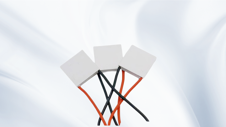
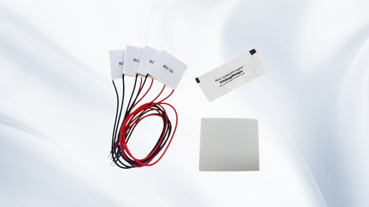
In today's advanced technological landscape, semiconductors are integral to systems that operate in harsh environments, such as space missions, nuclear reactors, and medical imaging equipment. These environments expose electronics to high levels of radiation, which can cause malfunctions, data corruption, or even catastrophic failures. To mitigate these risks, trustworthy semiconductor radiation fins have been developed as specialized heat dissipation components. Unlike standard fins, they are engineered with materials and designs that not only manage thermal loads but also provide radiation shielding and durability. This ensures that the semiconductors maintain their functionality and reliability over extended periods, even under intense radiation exposure.
Key Features and Design Principles
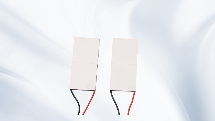
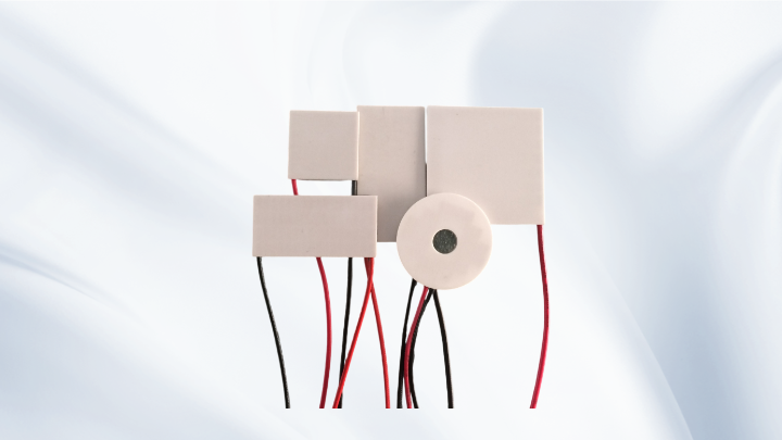
The effectiveness of trustworthy semiconductor radiation fins hinges on several key features. First, they are typically made from radiation-resistant materials such as aluminum alloys, copper, or specialized composites that can withstand ionizing radiation without degrading. These materials are chosen for their high thermal conductivity and ability to absorb or deflect radiation particles. Second, the design often includes enhanced surface areas and optimized geometries to maximize heat dissipation while minimizing weight and space usage. For instance, fin arrays may be structured to direct heat away from sensitive semiconductor junctions, reducing the risk of thermal runaway. Additionally, these fins undergo rigorous testing, including exposure to simulated radiation environments, to verify their performance and longevity. By integrating these principles, manufacturers can produce fins that meet stringent industry standards for reliability in critical applications.
Applications in High-Risk Industries
Trustworthy semiconductor radiation fins find applications across various high-risk industries where failure is not an option. In the aerospace sector, they are used in satellites and spacecraft to protect onboard electronics from cosmic radiation, which can cause single-event upsets or latch-up events. For example, in deep-space probes, these fins help maintain stable temperatures for processors and sensors, ensuring accurate data transmission over millions of miles. In nuclear energy, they are employed in control systems and monitoring equipment within reactors, where radiation levels are extremely high. Here, the fins prevent overheating and radiation damage, contributing to safe and efficient power generation. Similarly, in medical devices like MRI machines or radiation therapy equipment, they safeguard critical components from stray radiation, enhancing patient safety and device reliability. These real-world examples underscore the importance of investing in high-quality radiation fins to avoid costly downtime or safety hazards.
Common Challenges and Solutions
Despite their benefits, implementing trustworthy semiconductor radiation fins can present challenges. One common issue is material selection, as not all radiation-resistant materials offer optimal thermal properties. To address this, engineers often use hybrid approaches, combining materials like copper for conductivity with protective coatings for radiation shielding. Another challenge is cost and manufacturing complexity, as specialized designs and testing can drive up expenses. However, by leveraging advanced manufacturing techniques such as 3D printing or precision machining, companies can reduce costs while maintaining quality. Additionally, ensuring compatibility with existing semiconductor packages requires careful integration, which can be mitigated through modular designs and standardized interfaces. By anticipating these challenges and adopting proactive solutions, organizations can enhance the reliability of their systems without compromising on performance.
Best Practices for Implementation
To maximize the benefits of trustworthy semiconductor radiation fins, follow these best practices based on industry experience. Start by conducting a thorough risk assessment to identify the specific radiation threats and thermal requirements of your application. This will guide material and design choices, ensuring the fins are tailored to the environment. Next, collaborate with reputable suppliers who specialize in radiation-hardened components and can provide certifications or test data. During installation, ensure proper thermal interface materials, such as thermal pastes or pads, are used to optimize heat transfer between the semiconductor and the fin. Regular maintenance and monitoring are also crucial; implement periodic inspections to check for signs of wear or radiation damage, and replace fins as needed to prevent failures. By adhering to these guidelines, you can extend the lifespan of your electronics and maintain operational integrity in demanding settings.
Common Questions
What are the main differences between standard semiconductor fins and radiation fins?
Standard semiconductor fins are designed primarily for heat dissipation in typical environments, using common materials like aluminum. In contrast, radiation fins are engineered with radiation-resistant materials and enhanced designs to provide both thermal management and protection against ionizing radiation, making them suitable for harsh conditions like space or nuclear facilities.
How do I choose the right material for a radiation fin?
Select materials based on factors such as radiation resistance, thermal conductivity, and application-specific requirements. For high-radiation environments, alloys like aluminum 6061 or copper with protective coatings are often recommended. Consult with experts or refer to industry standards, such as those from NASA or nuclear regulatory bodies, for guidance.
Can radiation fins be used in consumer electronics?
Generally, radiation fins are not necessary for consumer electronics, as these devices operate in low-radiation environments. They are reserved for specialized applications where radiation exposure is a significant risk, such as in aerospace or medical equipment, to ensure reliability and safety.
What testing is involved for trustworthy semiconductor radiation fins?
Testing typically includes thermal cycling, radiation exposure simulations (e.g., using gamma rays or neutron beams), and mechanical stress tests to verify durability and performance. Compliance with standards like MIL-STD-883 or ISO certifications may also be required, depending on the industry.
Related Posts