


Production process
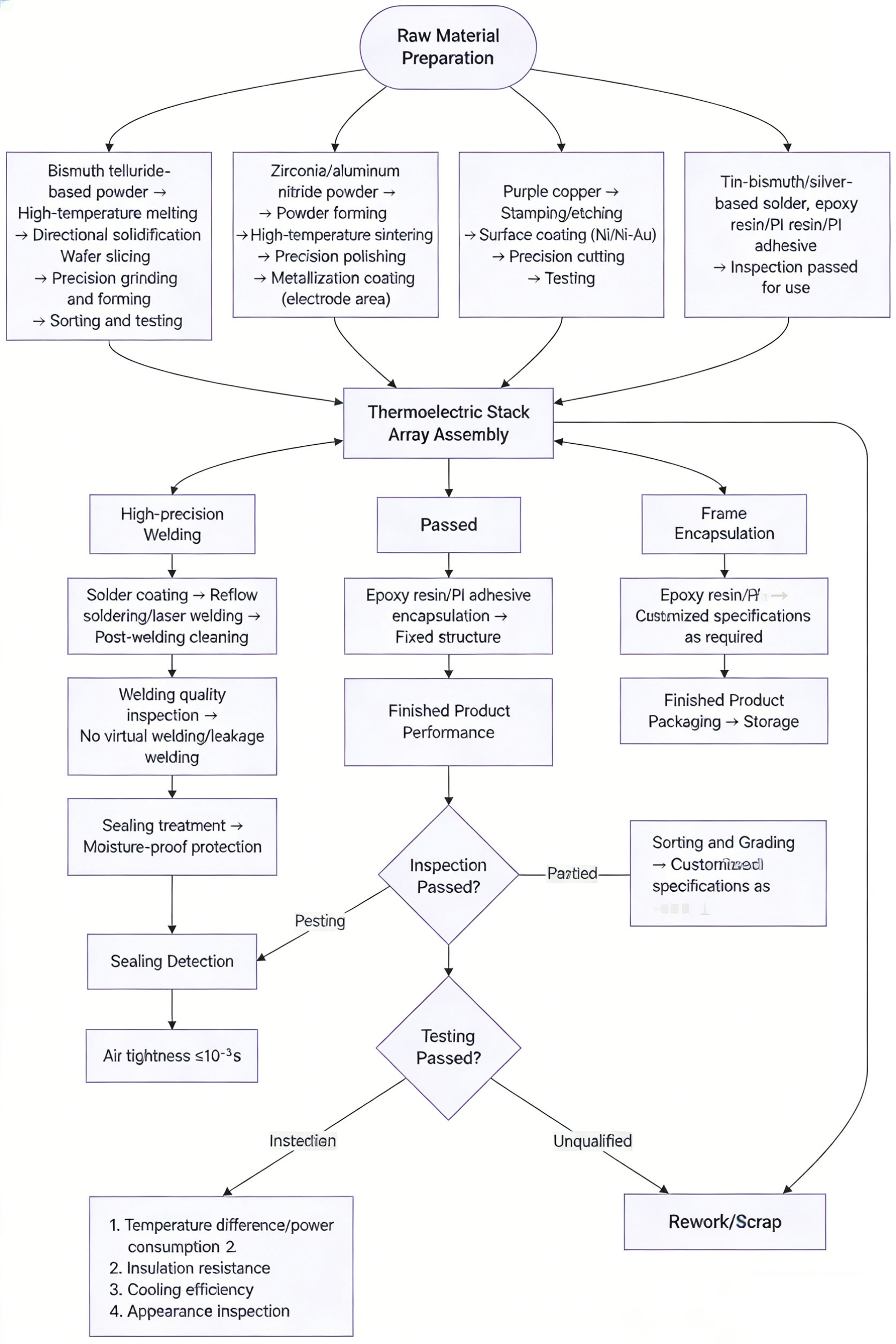
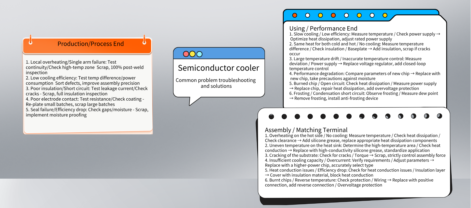
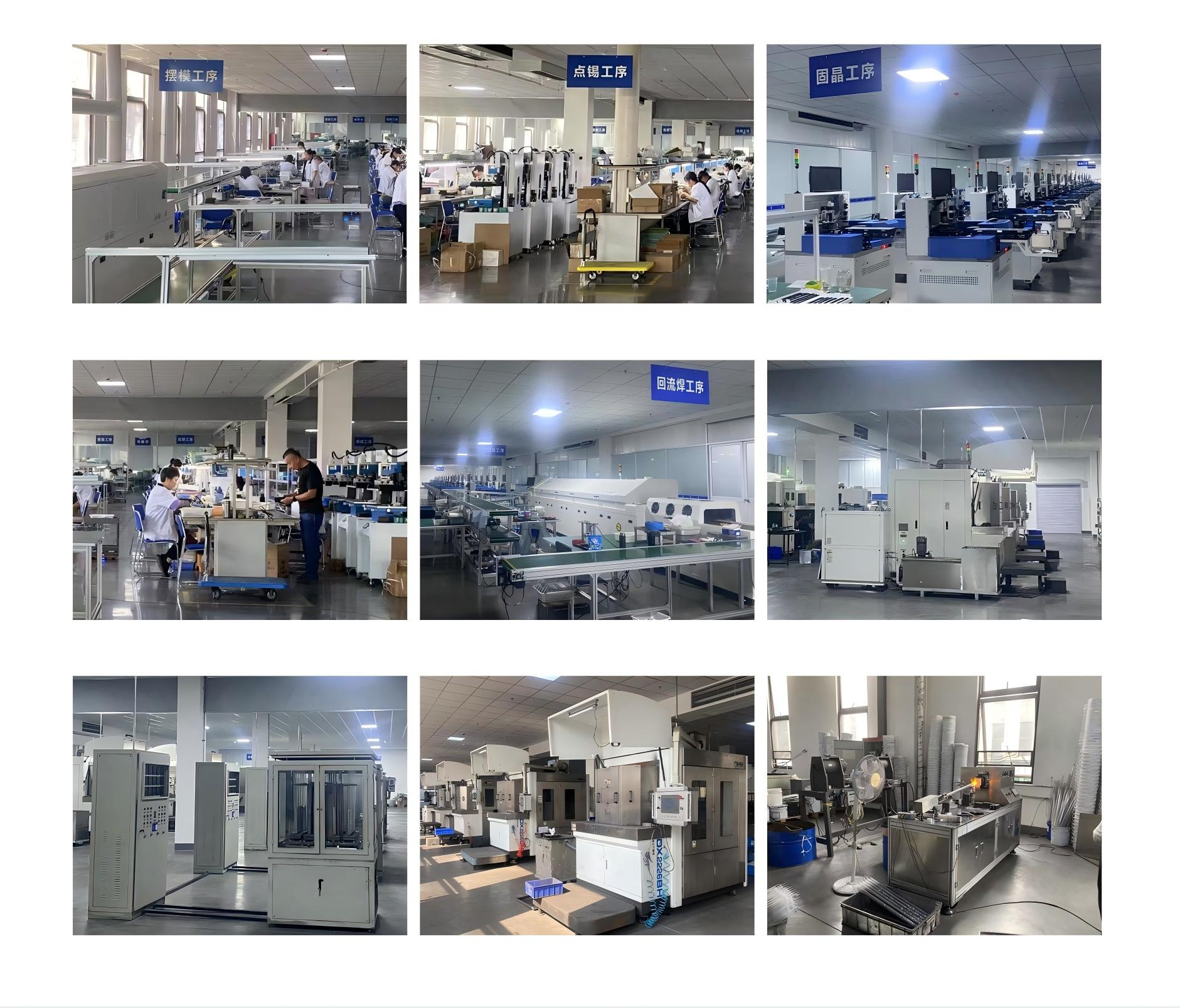
1. Raw material preparation: Bismuth telluride is the main material, with antimony/seelenium as the dopant. Combined with the specified substrate and copper conductor, it is processed through vacuum melting and directional solidification to produce N/P type ingots; the substrate and the flow guide component are clean and free of impurities, and the flow guide component is protected against oxidation. 2. Steel ingot processing: N/P type steel ingots undergo annealing to relieve internal stress, are precisely cut into standard grains, and unqualified products are screened out. 3. Substrate metallization: The ceramic substrate is equipped with copper/nickel/gold electrodes. Low-melting-point solder paste is applied through sputtering/electroplating to form multi-layer electrodes. High-precision printing is employed, ensuring no missed or false printing of the pads. 4. PN crystal grain arrangement: The automated equipment arranges N/P type crystals alternately on the substrate with solder pads, forming a thermoelectric stack array with precise positioning without any offset. 5. Reflow Soldering: The upper and lower substrates are welded to form a crystal array. The temperature is controlled in two stages for curing to prevent damage; after soldering, ultrasonic cleaning is used to remove residues, and hot air drying is performed. 6. Terminal Outlets: Ultrasonic/laser welding of wires to positive/negative connection terminals to ensure good conductivity and no false soldering. 7. Packaging protection: Apply heat-resistant glue to the edges and connection points to enhance protection; Mark the model, specifications, and production date with inkjet printing. 8. Finished product inspection: Test the cooling capacity, temperature difference, and insulation resistance. After undergoing cold and hot cycle/vibration tests, qualified products will be packaged with anti-static and moisture-proof measures and then stored in the warehouse