


Premium Semiconductor Radiation Fin: Enhancing Performance and Reliability in High-Tech Applications
What is a Premium Semiconductor Radiation Fin?
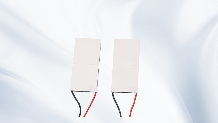
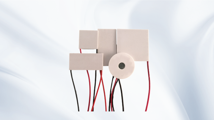
A Premium Semiconductor Radiation Fin is a specialized component integrated into semiconductor devices to enhance thermal management and mitigate radiation effects. Unlike standard fins, which primarily focus on heat dissipation, this premium version incorporates advanced materials like silicon carbide or gallium nitride, along with radiation-hardened designs. It works by increasing the surface area for heat transfer, while also shielding sensitive electronic parts from ionizing radiation, such as that encountered in space or nuclear environments. This dual functionality makes it indispensable for applications where reliability and performance are paramount, preventing overheating and radiation-induced failures that can compromise system integrity.
Key Features and Benefits
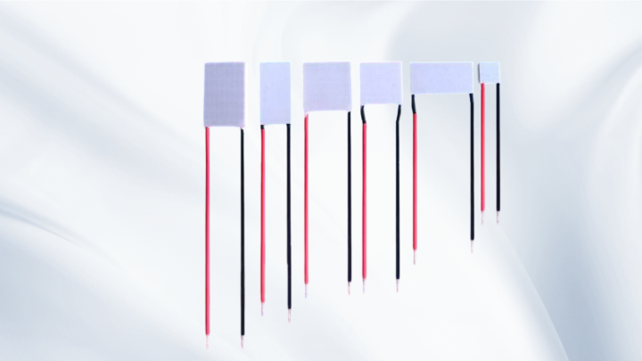
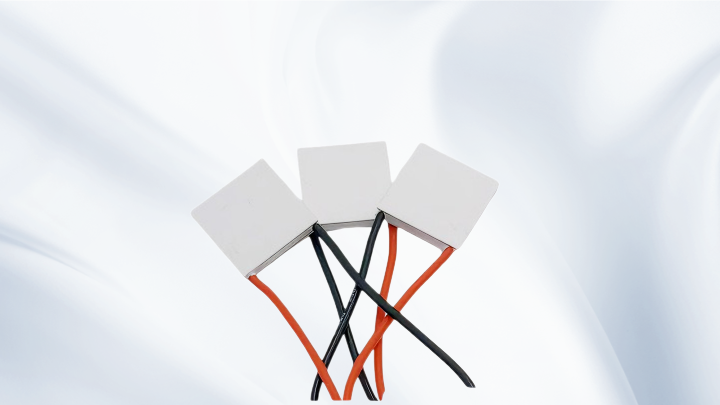
The Premium Semiconductor Radiation Fin offers several standout features that set it apart from conventional alternatives. Firstly, its use of high-quality materials ensures superior thermal conductivity, allowing for efficient heat dissipation even under extreme loads. This reduces the risk of thermal throttling, which can degrade performance in devices like processors or power electronics. Secondly, the radiation-hardened design provides robust protection against cosmic rays, gamma rays, and other forms of ionizing radiation, which can cause data corruption or permanent damage in sensitive circuits. Additionally, these fins are often engineered for durability, with resistance to corrosion and mechanical stress, extending the lifespan of semiconductor devices. From a practical perspective, this translates to enhanced reliability in critical systems, lower maintenance costs, and improved overall efficiency, making them a valuable investment for industries that demand high uptime and safety standards.
Applications in Various Industries
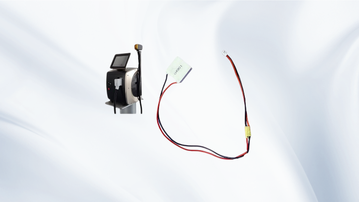
The versatility of the Premium Semiconductor Radiation Fin makes it applicable across a wide range of sectors. In the aerospace industry, for example, satellites and spacecraft rely on these fins to manage heat generated by onboard electronics while protecting against space radiation, ensuring mission success in harsh conditions. In medical devices, such as MRI machines or radiation therapy equipment, they help maintain precise temperature control and shield sensitive components from stray radiation, contributing to patient safety and accurate diagnostics. The automotive sector, particularly in electric vehicles and autonomous driving systems, uses these fins to handle high power loads and prevent overheating in battery management systems. Furthermore, in data centers and high-performance computing, they enable more efficient cooling solutions, allowing for denser server configurations and reduced energy consumption. By addressing specific challenges in each field, these fins support innovation and progress in technology-driven environments.
Design and Manufacturing Considerations
Creating an effective Premium Semiconductor Radiation Fin involves careful design and manufacturing processes. Engineers must balance factors such as material selection, fin geometry, and integration with existing semiconductor architectures. Advanced materials like silicon carbide are preferred for their high thermal conductivity and radiation resistance, but they can be costly, so cost-benefit analyses are crucial. The fin's shape, including aspects like thickness, spacing, and surface area, is optimized through simulations and testing to maximize heat dissipation without adding excessive weight or bulk. Manufacturing techniques, such as precision machining or additive manufacturing, ensure high-quality production with minimal defects. In my experience, collaborating with cross-functional teams, including materials scientists and thermal engineers, is key to developing fins that meet stringent performance criteria. Regular testing under simulated radiation and thermal conditions helps validate designs before deployment, reducing the risk of failures in real-world applications.
Common Questions
How does a Premium Semiconductor Radiation Fin differ from a standard heat sink?
A standard heat sink primarily focuses on dissipating heat through convection and conduction, often using materials like aluminum. In contrast, a Premium Semiconductor Radiation Fin combines thermal management with radiation shielding, using advanced materials and designs to protect against ionizing radiation, making it suitable for high-risk environments like space or medical settings.
What are the main challenges in implementing these fins?
The main challenges include high material costs, complex integration with existing semiconductor packages, and the need for specialized testing to ensure radiation hardness. Additionally, balancing performance with size and weight constraints can be difficult, especially in compact devices.
Are there any alternatives to Premium Semiconductor Radiation Fins?
Yes, alternatives include passive cooling methods like fans or liquid cooling systems, and other radiation-hardened components. However, these may not offer the same integrated benefits, and Premium Semiconductor Radiation Fins are often preferred for their dual functionality and reliability in critical applications.
Related Posts