


Industry-Leading Semiconductor Radiation Fin Technology: Enhancing Reliability in Harsh Environments
Understanding Semiconductor Radiation Fin Technology
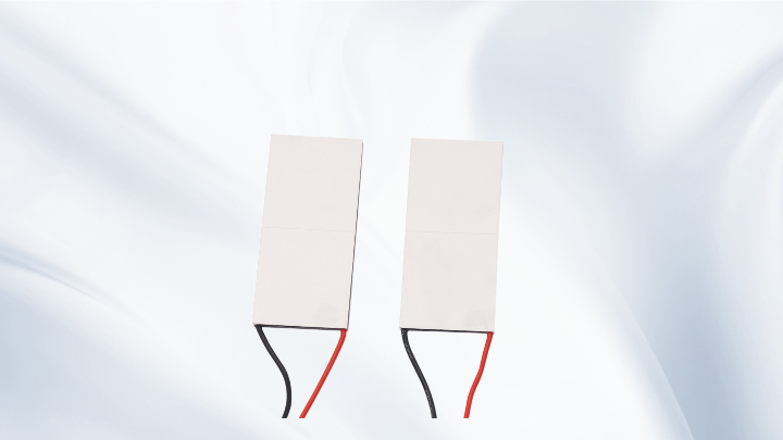
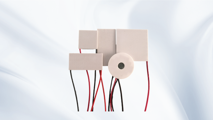
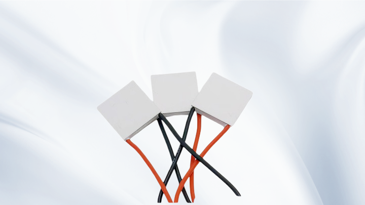
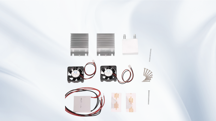
Semiconductor radiation fin technology refers to specialized design features, such as fins or shielding structures, integrated into semiconductor devices to mitigate the effects of ionizing radiation. These fins are typically made from materials like silicon carbide or advanced polymers that absorb or deflect radiation particles, preventing them from disrupting the device's electrical properties. This technology is crucial for applications where exposure to cosmic rays, gamma rays, or other radiation sources is common, as it helps maintain long-term reliability and functionality in harsh environments.
Key Principles and Design Innovations
The core principle behind radiation fins involves creating physical barriers that reduce radiation flux reaching the semiconductor's active regions. Innovations in this field include multi-layered fin structures that combine different materials for optimal protection, as well as miniaturized designs that fit within compact electronic systems. For example, in space missions, satellites use radiation-hardened chips with fins to withstand solar flares. Additionally, advanced simulation tools are employed to model radiation effects and optimize fin geometry, ensuring maximum efficiency without compromising performance.
Applications in High-Risk Industries
This technology finds widespread use in industries where radiation exposure is a constant threat. In aerospace, it protects avionics systems in aircraft and spacecraft from cosmic radiation, reducing the risk of system failures. In medical devices, such as MRI machines and radiation therapy equipment, radiation fins safeguard sensitive electronics, ensuring accurate diagnostics and treatments. The nuclear power sector also relies on these semiconductors for control systems in reactors, where they help prevent malfunctions caused by neutron bombardment. By integrating radiation fins, companies can achieve higher safety standards and operational uptime.
Benefits and Performance Advantages
The adoption of industry-leading radiation fin technology offers numerous benefits. It extends the lifespan of semiconductor devices by reducing degradation from radiation damage, which can lead to costly replacements. Performance-wise, it minimizes soft errors and data corruption, crucial for critical systems like autonomous vehicles or defense equipment. Moreover, it supports compliance with stringent regulatory requirements in sectors like healthcare and energy. From a cost perspective, while initial investment may be higher, the long-term savings from reduced maintenance and downtime make it a cost-effective solution for high-stakes applications.
Implementation Strategies and Best Practices
To effectively implement radiation fin technology, engineers should start with a thorough risk assessment to identify radiation exposure levels in their specific environment. Collaborating with semiconductor manufacturers who specialize in radiation-hardened designs is essential, as they can provide custom solutions. Best practices include regular testing under simulated radiation conditions to validate performance and incorporating redundancy in critical systems. For instance, using multiple fins in parallel can enhance protection. It's also important to stay updated with emerging materials and techniques, such as graphene-based fins, which offer improved shielding with lighter weight.
Common Questions
What is the primary function of a radiation fin in semiconductors?
The primary function is to shield the semiconductor's sensitive components from ionizing radiation, preventing disruptions like latch-up or leakage currents that can cause device failure.
How does radiation fin technology differ from traditional shielding methods?
Unlike bulky external shields, radiation fins are integrated directly into the semiconductor design, offering more compact and efficient protection with minimal impact on device size and weight.
Are there any limitations to using radiation fins?
Yes, limitations include potential increases in manufacturing complexity and cost, as well as the need for specialized materials that may have thermal or electrical constraints in some applications.
Related Posts